Modulation basics, part 1: Amplitude and frequency modulation. Modulation is perhaps one of the most complicated things that I have to explain in my one-day Tech class. Perhaps if I could get my students to read this article before I try to explain it, they would understand it a bit more.

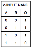
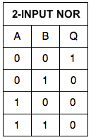
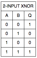
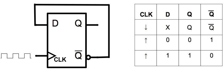
How to Read Datasheets: Logic ICs. This is #5 in a series of articles on digital ICs. This particular articles discusses the evolution of complementary metal-oxide semiconductor (CMOS) technology and how CMOS technology differs from transistor-transistor logic (TTL) technology.
10 Best Single Board Computers for 2018. Arduinos and Raspberry Pis are all the rage in amateur radio, but there are a number of other single-board computers that might be worth looking at for your amateur radio projects.