
As of July 1, 2020, this post will be obsolete. See the corresponding post from my 2020 version of No Nonsense Extra Class License Study Guide.
While transistor theory is outside the scope of this study guide, I will attempt to at least give you a basic understanding of how transistors are put together and how they work. For more information, take a look at these two links:
Most transistors we use in amateur radio are made of silicon. Silicon is a semiconductor. That is to say, it’s neither a conductor with a very low resistance, like copper, or an insulator with a very high resistance, like plastic or glass.
You can manipulate the electrical characteristics of silicon by adding slight amounts of impurities to a pure silicon crystal. When transistor manufacturers add an impurity that adds free electrons to the silicon crystal, it creates a crystal with a negative charge. We call that type of silicon N-type silicon. N-type is a semiconductor material that contains excess free electrons. (E6A02) In N-type semiconductor material, the majority charge carriers are the free electrons. (E6A16)
When you add other types of impurities to a pure silicon crystal, you can create a crystal with a positive charge. We call this type of material P-type semiconductor material. The majority charge carriers in P-type semiconductor material are called holes. P-type is the type of semiconductor material that contains an excess of holes in the outer shell of electrons. (E6A15)
You can think of them as holes as spots in the crystal that accepts free electrons into. Because of that, the name given to an impurity atom that adds holes to a semiconductor crystal structure is call an acceptor impurity. (E6A04)
Silicon isn’t the only semiconductor material used to make transistors. At microwave frequencies, gallium arsenide is used as a semiconductor material in preference to germanium or silicon. (E6A01)
Semiconductor diodes
Diodes are the simplest semiconductor devices. A PN junction diode is formed when you join a bit of P-type material to a bit of N-type material. When you join the two materials, some electrons from the N-type material migrate over to the P-type material and fill holes there. As a result, holes form in the N-type material. This migration of charge forms what is called the depletion region at the PN junction, and an electric field forms across this region. The electric field generates a voltage across the junction.
The most important characteristic of a PN junction diode is that it only allows current to flow when it is forward-biased, that is to say when the voltage applied to the P-type material is more positive than the voltage applied to the N-type material. When a PN junction diode is reversed biased—that is when the voltage applied to the P-type material is more negative than the voltage applied to the N-type material—the diode will not conduct current. A PN-junction diode does not conduct current when reverse biased because holes in P-type material and electrons in the N-type material are separated by the applied voltage, widening the depletion region. (E6A03) This makes it impossible for current to flow through the region
Bipolar junction transistors
Perhaps the most popular type of transistor is the bipolar junction transistor (BJT). Bipolar junction transistors are three-terminal devices, called the emitter, base, and collector. In an NPN transistor, the emitter and collector are N-type material and the base is P-type material. In a PNP transistor, the emitter and collector are P-type, while the base is N-type. The base is sandwiched between the collector and emitter, so there is a diode junction between the base and the collector and the base and emitter. The circuit diagrams for these transistors are shown below.
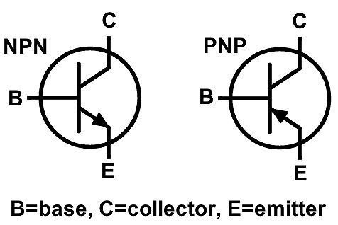
When the base-emitter diode is forward-biased, a current, called the base current will flow. A silicon NPN junction transistor is biased on when the base-to-emitter voltage of approximately 0.6 to 0.7 volts. (E6A07)
If there is an appropriate voltage between the collector and emitter, this small base current will cause a much larger current to flow between the collector, through the base to the emitter. The amount of base current controls how much collector current flows. This is how transistors amplify signals.
The change in collector current with respect to base current is the beta of a bipolar junction transistor. (E6A06) This is also sometimes called the hfe, or current gain, of a transistor. The change of collector current with respect to emitter current is the alpha of a bipolar junction transistor. (E6A05)
Another important characteristic of a bipolar transistor is the alpha cutoff frequency. This is a measure of how high in frequency a transistor will operate. Alpha cutoff frequency is the frequency at which the grounded-base current gain of a transistor has decreased to 0.7 of the gain obtainable at 1 kHz. (E6A08)
Field effect transistors
A field-effect transistor (FET) is a device that uses an electric field to control current flow through the device. Like the bipolar transistor, a FET normally has three terminals. The names of the three terminals of a field-effect transistor are gate, drain, source. (E6A17)
FETs are normally made with a technology called Complementary Metal-Oxide Semiconductor, or CMOS. The initials CMOS stand for Complementary Metal-Oxide Semiconductor. (E6A13) FETs made with CMOS technology are sometimes call MOSFETs.
In Figure E6-2 (below), schematic symbol 1 is the symbol for a P-channel junction FET. (E6A11) In Figure E6-2 (below), schematic symbol 4 is the symbol for an N-channel dual-gate MOSFET. (E6A10)
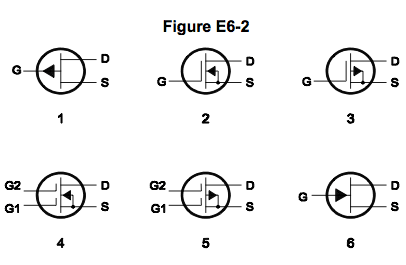
One characteristic of the MOSFET is that they have a high input impedance. This makes them more attractive for use in many test equipment applications than bipolar transistors. How does DC input impedance at the gate of a field-effect transistor compare with the DC input impedance of a bipolar transistor? An FET has high input impedance; a bipolar transistor has low input impedance. (E6A14)
One disadvantage of using MOSFETs is that they are very sensitive to electrostatic discharge (ESD). Sometimes, they are damaged by static discharges so low that you never even see the spark or feel the shock. To reduce the chance of the gate insulation being punctured by static discharges or excessive voltages many MOSFET devices have internally connected Zener diodes on the gates. (E6A12)
Most FETs are enhancement-mode devices. When using an enhancement-mode FET, you must apply a voltage to the gate to get current to flow from source to drain. Some FETs are, however, depletion mode devices. A depletion-mode FET is an FET that exhibits a current flow between source and drain when no gate voltage is applied. (E6A09)
Leave a Reply