
• Skip to primary navigation
  • Skip to main content
  • Skip to primary sidebar
  • Skip to footer

KB6NU's Ham Radio Blog

KB6NU's Ham Radio Blog
  • HOME
  • Study Guides
  • Teach a One-Day Tech Class
  • W8SRC Repeater Guide
  • Advertise
  • Hire Me

Extra Class question of the day: Digital integrated circuits

September 10, 2012 By Dan KB6NU Leave a Comment

Integrated circuits (ICs) are now an integral part (pun intended) of amateur radio electronics. The two main technologies used to manufacture IC are transistor-transistor logic, or TTL, and complementary metal-oxide semiconductor, or CMOS.

CMOS is arguably the most common type of digital IC. An advantage of CMOS logic devices over TTL devices is that the have lower power consumption. (E6C05) CMOS digital integrated circuits also have high immunity to noise on the input signal or power supply because the input switching threshold is about one-half the power supply voltage. (E6C06)

TTL is the other common digital logic IC technology. 5 volts is the recommended power supply voltage for TTL series integrated circuits. (E6C01) The inputs of a TTL device assume a logic-high state if they are left open. (E6C02)

BiCMOS logic is an integrated circuit logic family using both bipolar and CMOS transistors. (E6C12) An advantage of BiCMOS logic is that it has the high input impedance of CMOS and the low output impedance of bipolar transistors. (E6C13)

Tri-state logic devices are logic devices with 0, 1, and high impedance output states. (E6C03) These devices can be made with either TTL or CMOS technology. The primary advantage of tri-state logic is the ability to connect many device outputs to a common bus. (EC604) When a device’s outputs are in the high-impedance state, they act as if they are disconnected.
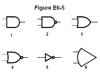
Digital Logic Schematic Symbols

When working with digital ICs, it is important to recognize the various symbols for the different types of logic gates. In Figure E6-5, 1 is the schematic symbol for an AND gate. (E6C07) In Figure E6-5, 2 is the schematic symbol for a NAND gate. (E6C08) In Figure E6-5, 3 is the schematic symbol for an OR gate. (E6C09) In Figure E6-5, 4 is the schematic symbol for a NOR gate. (E6C10) In Figure E6-5, 5 is the schematic symbol for the NOT operation (inverter). (E6C11)

Related posts:

  1. 2020 Extra Class study guide: E6C – Digital ICs: Families of digital ICs; gates; Programmable Logic Devices (PLDs)
  2. 2016 Extra Class study guide: E6C – Digital ICs
  3. Extra Class question of the day: field-effect transistors
  4. Extra Class question of the day: digital circuits, flip-flops

Filed Under: Digital Logic, Electronic Components, Extra Class Question of the Day

Reader Interactions

Leave a Reply Cancel reply

Your email address will not be published. Required fields are marked *

This site uses Akismet to reduce spam. Learn how your comment data is processed.

Primary Sidebar

No Nonsense Technician Class License Study Guide (for tests given between July 2026 and June 2030)

New No Nonsense Technican Class Study Guide now available!

The 2026 version of my Tech Class study guide is now available, and as always, the PDF version is FREE!. The ePub version costs $11.97, and a Kindle version and paperback version will be available on Amazon shortly.

Click here to get all of my "No Nonsense" study guides.

Also available: The CW Geek's Guide to Having Fun with Morse Code

W5SWL.Com
Retevis Ailunce H1 DMR Radio
DXpander: Cobweb antennas, Laser Cutting

You’ve got mail!

Enter your email address below and get an email every time I publish a new post.

Email


I frequently teach classes to help newcomers get their licenses. The next class will take place on Saturday, October 10, 2026 on the University of Michigan campus. Click here for more information.

If you can't make the class, subscribe to the mailing list to be notified of when the next class will be held.

You can always download my free study guide, and if you have any questions about the classes, or amateur radio in general, please feel free to email me directly.

Support KB6NU.Com

Donate $7.30 and get two of these cool stickers. Measuring 4.25-in. W by 2.75-in. H, it's perfect for your car, your shack, or wherever!

Contact me

If you have a question or comment about one of my blog posts, or a question about any of the material in my study guides, or just a question about ham radio in general, you can email me at [email protected].

Blogs You Should Also Read

  • AE5X: A CW-centric blog from Kingswood, Texas
  • K0LWC Blog
  • LA3ZA Ham Radio Blog
  • Little Radios, Big Fun – WB3GCK
  • Mr. Vacuum Tube's Blog
  • Radio Artisan – K3NG
  • The K0NR Weblog
  • VE3WDM's QRP Ham Radio Blog
  • W2LJ’s Blog

Ham Radio Websites

  • Dashtoons – The Hammin' Comedy by Jeff K1NSS

Podcasts

  • ICQ Podcast
  • Linux in the Ham Schack
  • No Nonsense Amateur Radio Podcast
  • Resonant Frequency Amateur Radio Podcast

Recent Comments

  • mike on Instant Character Recognition is the key to CW speed
  • Matt W1CDN on A completely different picture of Wayne Green, W2NSD (SK)
  • Chana Walsh on Rethinking ham radio education
  • Rob WfourZNG on Videos: What’s next for POTA, ham radio helps rescue man trapped in cave
  • Dan KB6NU on The EMF Explorer: A badge for ham radio?

Meta

  • Log in
  • Entries feed
  • Comments feed
  • WordPress.org

Footer

Copyright © 2026 Daniel M. Romanchik, KB6NU · Log in